How To Design A Pcb From A Schematic. After you’ve done one project, you’ll know the basics and can design more pcbs on your own. before you start designing your pcb, it’s a good idea to make a schematic of your circuit. transfer data from a pcb schematic into a new pcb layout using altium designer. The schematic will serve as a. All you need to do is to solder the components to the board, just like a soldering kit, and your circuit should work. I’ll show you by creating a super simple project in kicad. In this kicad tutorial, you’ll learn how to make your first pcb. in this article, you will learn the basics of how to plan a schematic for a custom pcb and lay out. before you create a layout, you need to create a schematic that includes the components your system needs and shows connections between them. It is the first step of electronic product design. a pcb schematic is a logical and visual representation of an electrical circuit.
from pcbways.pages.dev
a pcb schematic is a logical and visual representation of an electrical circuit. I’ll show you by creating a super simple project in kicad. before you start designing your pcb, it’s a good idea to make a schematic of your circuit. All you need to do is to solder the components to the board, just like a soldering kit, and your circuit should work. It is the first step of electronic product design. before you create a layout, you need to create a schematic that includes the components your system needs and shows connections between them. The schematic will serve as a. in this article, you will learn the basics of how to plan a schematic for a custom pcb and lay out. transfer data from a pcb schematic into a new pcb layout using altium designer. After you’ve done one project, you’ll know the basics and can design more pcbs on your own.
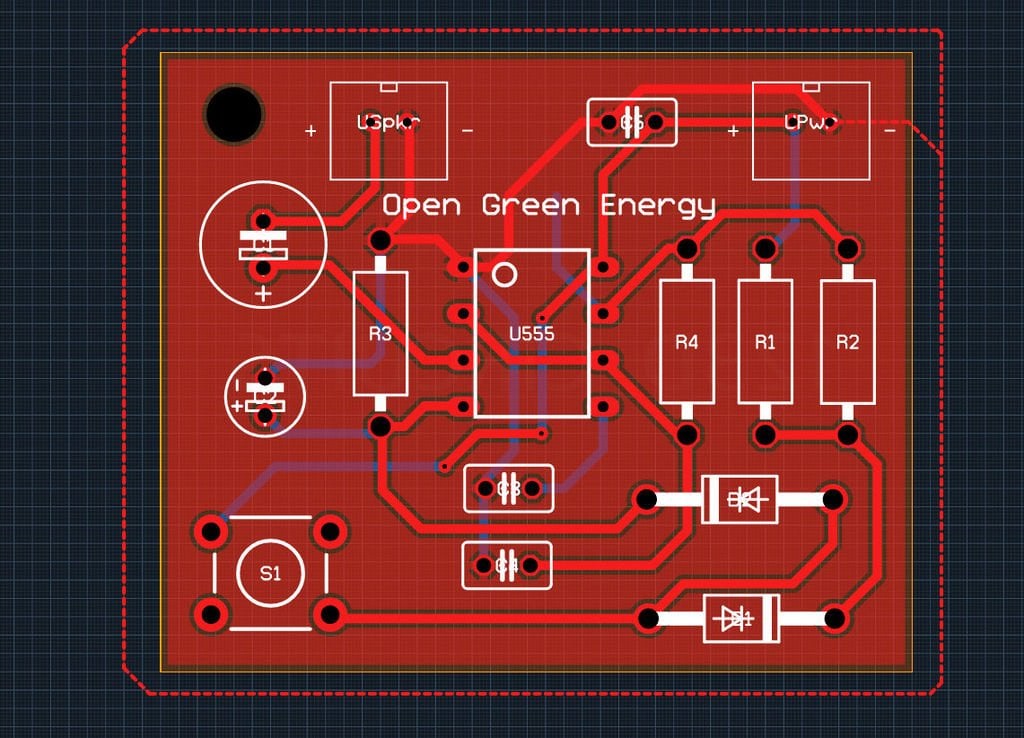
simple circuit diagram for pcb Circuit diagram before pcb design
How To Design A Pcb From A Schematic before you create a layout, you need to create a schematic that includes the components your system needs and shows connections between them. before you create a layout, you need to create a schematic that includes the components your system needs and shows connections between them. The schematic will serve as a. in this article, you will learn the basics of how to plan a schematic for a custom pcb and lay out. All you need to do is to solder the components to the board, just like a soldering kit, and your circuit should work. transfer data from a pcb schematic into a new pcb layout using altium designer. It is the first step of electronic product design. before you start designing your pcb, it’s a good idea to make a schematic of your circuit. After you’ve done one project, you’ll know the basics and can design more pcbs on your own. I’ll show you by creating a super simple project in kicad. a pcb schematic is a logical and visual representation of an electrical circuit. In this kicad tutorial, you’ll learn how to make your first pcb.